

As a reliable erbium oxide supplier, I've often been asked about the potential applications of erbium oxide in semiconductor devices. In this blog post, I'll delve into the properties of erbium oxide and explore whether it can be used in semiconductor devices.

Properties of Erbium Oxide
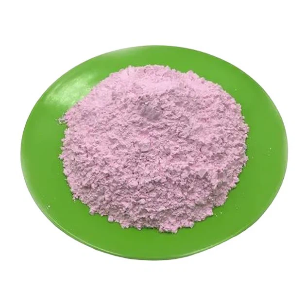
Erbium oxide (Er₂O₃), also known as erbia, is a rare - earth compound with several notable properties. It has a high melting point, typically around 2346 °C, which gives it excellent thermal stability. This compound has a characteristic pink - red color in its pure form.
One of the most important properties of erbium oxide is its optical properties. It has sharp and well - defined absorption and emission bands in the near - infrared region. These optical properties make it attractive for applications in photonics, where precise control of light is required.
From an electrical perspective, erbium oxide is an insulator. It has a relatively high dielectric constant, which means it can store electrical energy efficiently when an electric field is applied. This property is crucial in many semiconductor - related applications, as it can be used to create capacitors and other energy - storage components.
Potential Applications in Semiconductor Devices
Optical Amplifiers
In the field of optical communication, erbium - doped fiber amplifiers (EDFAs) are widely used. Although in EDFAs, erbium ions are typically doped into silica fibers rather than using erbium oxide directly, the principle is closely related. Erbium has unique energy levels that allow it to absorb photons at a certain wavelength and then re - emit them at a longer wavelength, amplifying the optical signal. In semiconductor - based optical communication systems, erbium oxide could potentially be integrated into semiconductor - based waveguides. For example, by depositing erbium oxide thin films on semiconductor substrates, it may be possible to create on - chip optical amplifiers. This would greatly enhance the performance of optical communication chips, allowing for higher - speed data transmission over longer distances. More information about high - quality erbium oxide for such potential applications can be found on our Erbium Oxide Powder page.
Gate Dielectrics
As semiconductor devices continue to shrink in size, traditional silicon dioxide gate dielectrics face limitations such as high leakage currents. High - k dielectric materials are being explored as alternatives. Erbium oxide has a relatively high dielectric constant, which makes it a potential candidate for gate dielectric applications. A high - k dielectric can reduce the leakage current while maintaining good capacitance, which is essential for the proper functioning of transistors. By using erbium oxide as a gate dielectric, semiconductor manufacturers may be able to further scale down the size of transistors without sacrificing performance. Our Nano Erbium Oxide product may be particularly suitable for this application, as the nanoscale particles can provide better film - forming properties.
Photovoltaic Devices
In photovoltaic cells, the ability to absorb and convert light energy into electrical energy is crucial. Erbium oxide's optical absorption properties in the near - infrared region can be exploited to enhance the efficiency of photovoltaic devices. By incorporating erbium oxide into the semiconductor structure of a solar cell, it may be possible to capture more of the solar spectrum, especially the near - infrared part that is often not fully utilized by traditional semiconductor materials. This could lead to an increase in the overall power conversion efficiency of the solar cell.
Challenges and Limitations
Despite its potential, there are several challenges to using erbium oxide in semiconductor devices.
Compatibility with Semiconductor Processes
Semiconductor manufacturing processes are highly precise and require materials that can be easily integrated into existing fabrication techniques. Erbium oxide may not be fully compatible with some of the common semiconductor processes, such as etching and deposition. For example, finding the right etchant that can selectively remove erbium oxide without damaging the underlying semiconductor layers can be difficult. Additionally, depositing high - quality erbium oxide thin films with uniform thickness and composition on semiconductor substrates is a technical challenge.
Cost
Erbium is a rare - earth element, and the extraction and purification of erbium oxide can be expensive. This cost factor may limit its widespread use in semiconductor devices, especially in cost - sensitive applications. However, as the demand for high - performance semiconductor devices increases, the cost - effectiveness of using erbium oxide may improve over time.
Long - term Stability
In a semiconductor device, long - term stability is crucial. Erbium oxide may be subject to degradation over time due to factors such as temperature, humidity, and electrical stress. Ensuring that erbium - oxide - based components can maintain their performance over the lifetime of the semiconductor device is a significant challenge that needs to be addressed.
Our Offerings as an Erbium Oxide Supplier
As an erbium oxide supplier, we are committed to providing high - quality erbium oxide products for various applications, including potential semiconductor uses. Our erbium oxide products are carefully processed to ensure high purity and consistent quality. We offer different forms of erbium oxide, such as Erbium Oxide Glaze, powder, and nano - sized particles, to meet the diverse needs of our customers.
We also have a team of experts who can provide technical support and guidance on the use of erbium oxide in semiconductor applications. Whether you are researching new semiconductor device designs or looking to improve the performance of existing devices, we can work with you to find the most suitable erbium oxide products and solutions.
Conclusion
In conclusion, erbium oxide has significant potential for use in semiconductor devices. Its unique optical and electrical properties make it attractive for applications such as optical amplifiers, gate dielectrics, and photovoltaic devices. However, there are also challenges to overcome, including compatibility with semiconductor processes, cost, and long - term stability.
If you are interested in exploring the use of erbium oxide in your semiconductor projects, we invite you to contact us for further discussion. Our team is ready to assist you in understanding the best ways to incorporate our high - quality erbium oxide products into your semiconductor device designs. We believe that through collaboration and innovation, we can help unlock the full potential of erbium oxide in the semiconductor industry.
References
- "Handbook of Rare - Earth Element Chemistry and Applications"
- Research papers on semiconductor device materials and rare - earth compounds from academic journals such as "IEEE Transactions on Electron Devices" and "Journal of Applied Physics"
- Industry reports on the development of high - k dielectric materials for semiconductor applications.